Canon’s nanoimprint technology seeks to disrupt semiconductor manufacturing - 2 minutes read
Today, Canon made waves in the semiconductor world by announcing its new nanoimprint lithography systems for chip production. The company is positioning the technology as an alternative to the costly and complex extreme ultraviolet lithography (EUV) systems currently dominated by Dutch firm ASML Holding NV.
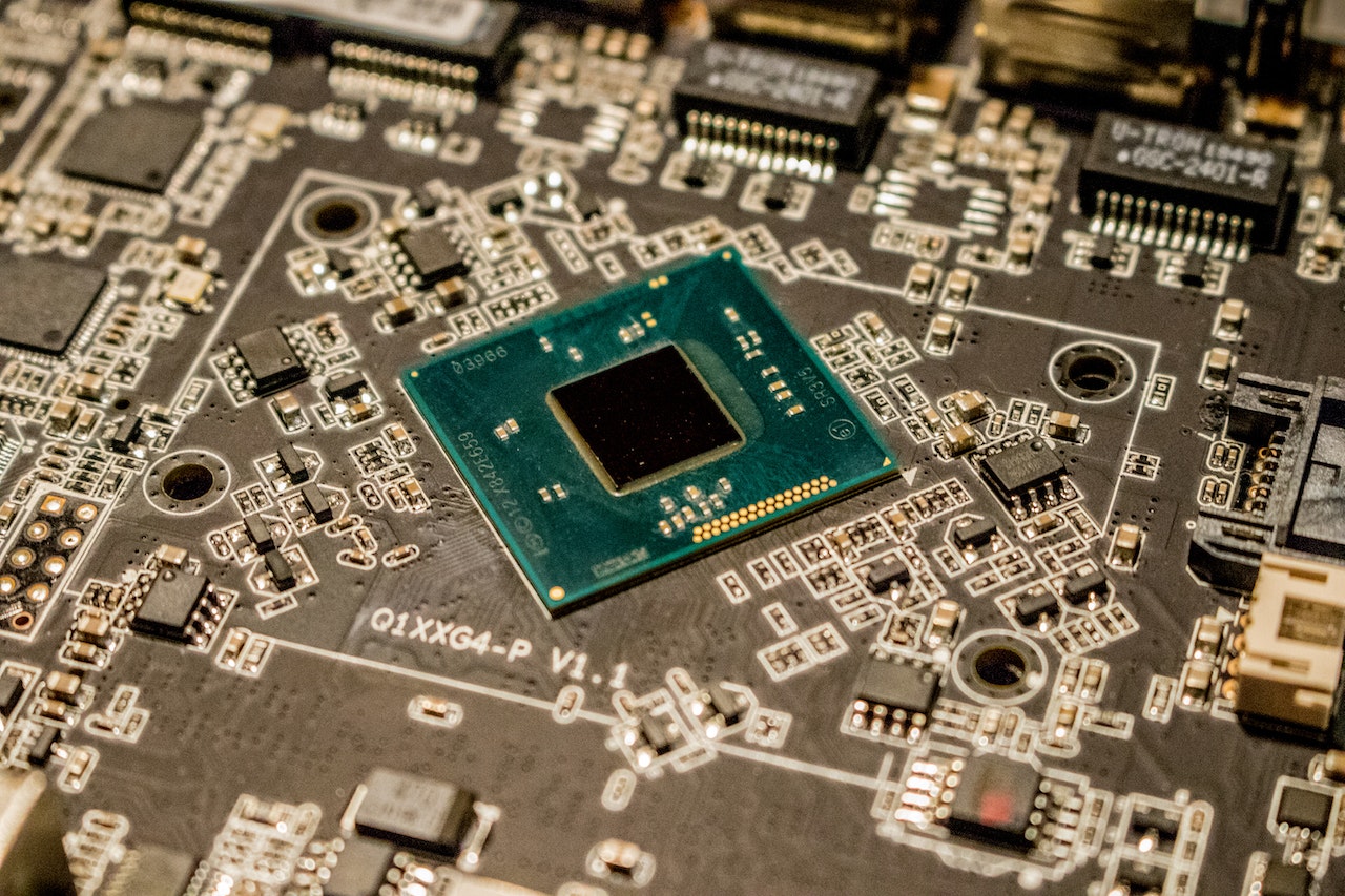
According to an Oct. 13 Canon announcement, the firm’s nanoimprint machines can produce 5nm chip circuits, matching the cutting-edge level of EUV. The company predicts enhancements to imprint materials and overlay alignment could improve resolution to 2nm, placing Canon decisively into next-generation manufacturing. This is a significant leap for the Japanese tech giant after lagging behind in the EUV race.
Unlike EUV’s sophisticated use of high-powered lasers, nanoimprinting imprints nanoscale circuit patterns directly onto silicon wafers using a mold-like stamp. Canon believes this simpler mechanical imprinting process will provide a cheaper and more accessible option for chipmakers.
Furthermore, according to Bloomberg the technology’s novelty may allow it to bypass current US export restrictions on EUV systems to China. A Canon spokesperson would not confirm whether the nanoimprint systems would be restricted to Bloomberg.
Nanoimprinting has long been touted as an alternative lithography solution despite past challenges with defects
But after acquiring nanoimprint pioneer Molecular Imprints Inc. in 2014, Canon has dedicated nearly a decade to developing the technology and solving these issues. With the commercial launch, Canon must now prove its nanoimprint systems can enable reliable high-volume manufacturing.
Canon’s rival Nikon Corp. has also struggled to keep pace as ASML dominates the lithography market. ASML has seen tremendous demand with five straight quarters of rising revenues and anticipates 30% net sales growth this year as chipmakers adopt EUV. Canon’s stock has also rallied 26% this year amid broader market gains.
The launch represents Canon’s first foray into cutting-edge lithography systems after years focused on less advanced equipment. This is underscored by the construction of its new semiconductor equipment plant in Utsunomiya to produce the nanoimprint systems. If successfully adopted, the technology could truly shake up an industry firmly entrenched in EUV and end ASML’s monopoly.
Featured Image Credit: Jeremy Waterhouse; Pexels; Thank you!
Radek Zielinski is an experienced technology and financial journalist with a passion for cybersecurity and futurology.
Source: ReadWrite
Powered by NewsAPI.org